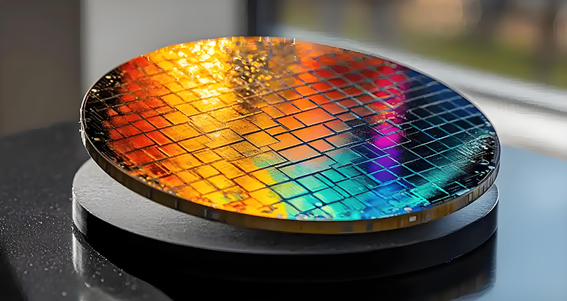
If rare earth magnets are the "muscles" of semiconductor equipment, then rare earth compounds are the "scalpels" in the processing stage. In the "transformation" of a wafer from a crude silicon wafer to a chip, every step of "carving" relies on the "precise operation" of rare earths. Chemical mechanical polishing (CMP) is the most typical example. When the surface of a wafer needs to achieve atomic-level flatness, traditional abrasives (such as silicon dioxide) rely on "brute force grinding", which is prone to scratching the wafer; while cerium dioxide (CeO₂) polishing agents use the dual effect of "chemical reaction + physical grinding", like an "intelligent eraser" to precisely remove impurities. In an alkaline environment, cerium ions (Ce³⁺/Ce⁴⁺) on the surface of CeO₂ react with silicon dioxide (SiO₂) to form soluble cerium silicate, achieving "selective removal" - the removal rate of SiO₂ is three times that of traditional abrasives, yet it hardly damages surrounding materials such as silicon nitride. Currently, over 90% of shallow trench isolation (STI) polishing processes worldwide use CeO₂ polishing agents, and a single 12-inch wafer polishing process requires the consumption of about 10 grams of high-purity CeO₂ (99.99% purity).
The "protective shield" of etching machines also relies on rare earths. During the etching process, fluorine plasma is as corrosive as "aqua regia", and ordinary quartz components will be eroded with holes in no time. However, a yttrium oxide (Y₂O₃) coating can form a "chemical barrier" on the surface of the component: yttrium (Y) oxide has extremely strong chemical stability and will form a dense yttrium fluoride (YF₃) protective layer in fluorine plasma, extending the component's lifespan from 3 months to over 1 year. The inner lining of advanced process etching machines from TSMC and Samsung is almost entirely coated with Y₂O₃ - this "rare earth anti-corrosion" approach currently has no alternative.
Even the inspection stage cannot do without rare earths. The core material of the laser used for wafer alignment is neodymium-doped yttrium aluminum garnet (Nd:YAG) crystal. Neodymium ions (Nd³⁺) can generate 1.064μm laser, which is converted into 355nm ultraviolet light to achieve nanometer-level alignment inspection. Without this laser, the wafer cannot be precisely "aligned" with the mask, and the chip yield would plummet by more than 90%.
Scan to wechat :
